
Plant watering system: my first PCB
Previously, I created a plant monitor that tracked soil moisture and sent notifications when the plant needed watering. But wouldn’t it be nice if it could water the plant instead of sending a notification? This new project does exactly that.
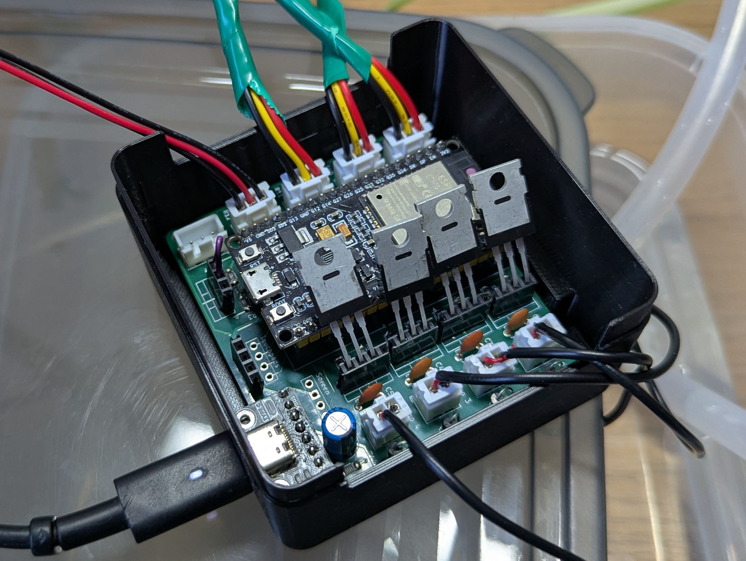
My plant watering system supports four plants, with a soil moisture sensor and a pump for each plant. The pumps draw water from a water tank, which contains a water level sensor. I’m using an ESP32 microcontroller for the brains, as it comes with Internet connectivity and low-power deep sleeping.
Why make a PCB? #
Why go through the effort of making a PCB when a quick protoboard or stripboard would have been quicker? I did originally make a stripboard but I found that they have terrible grounding properties. I wrote a blog post about it, but in summary, noise from the pumps interfered with the microcontroller and caused it to crash.
A PCB provides much better grounding than a protoboard or stripboard. It allows you to have a layer of the board dedicated to ground, called a ground plane. I watched an excellent video on this topic called How to Achieve Proper Grounding. It taught me a lot and I applied the lessons to my PCB design.
I was looking for an excuse to learn how to make PCBs, so I welcomed this opportunity.
PCB design #
Schematic and PCB #
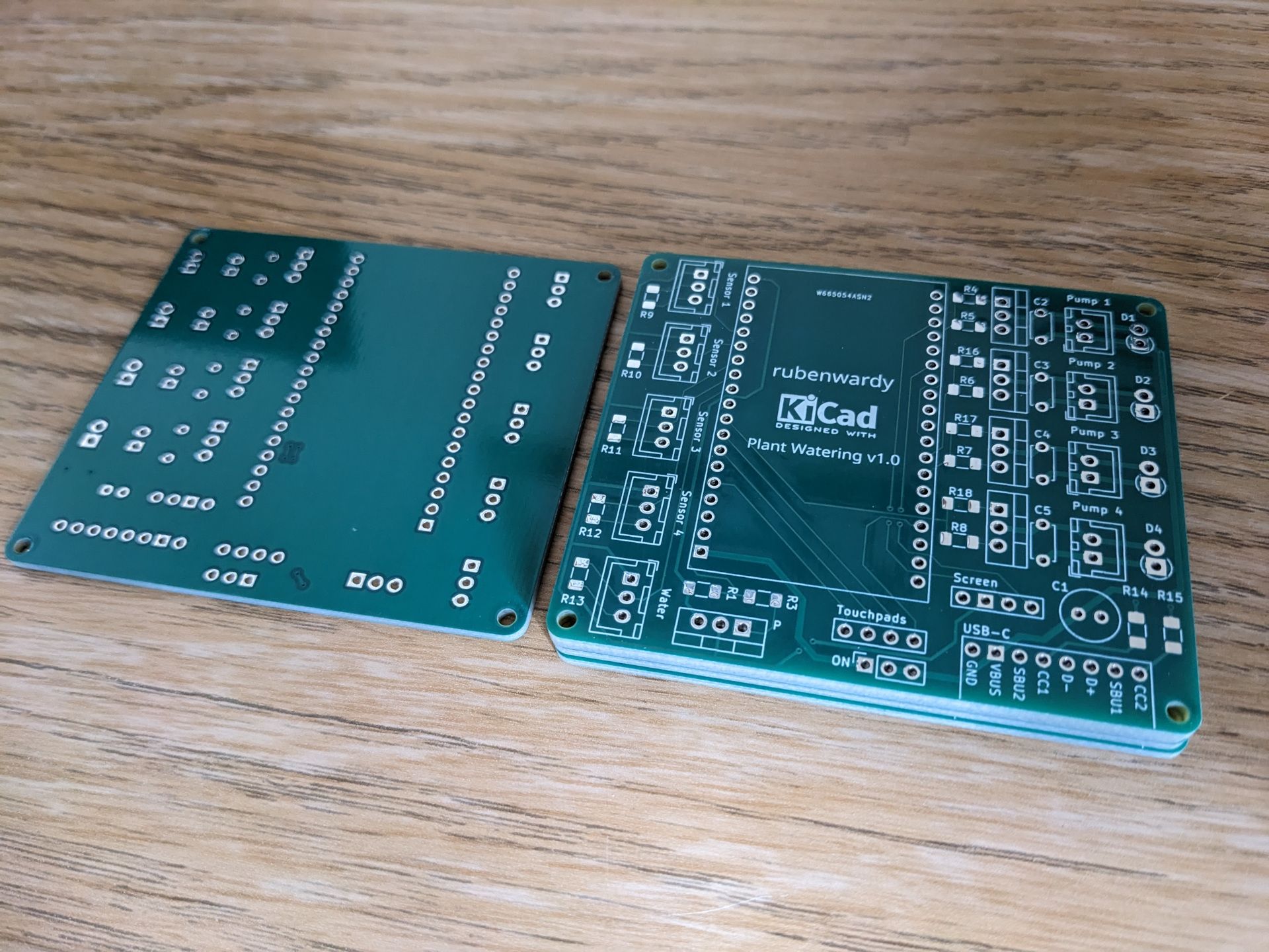
I designed my PCB using KiCAD, which is free and open-source. I learned how to use KiCAD by watching a tutorial by Phil’s Lab on YouTube.
There are two steps to designing a PCB. The first is to create a high-level diagram of your circuit called a schematic. The schematic allows you to specify an electrical circuit without worrying about how it will be built.
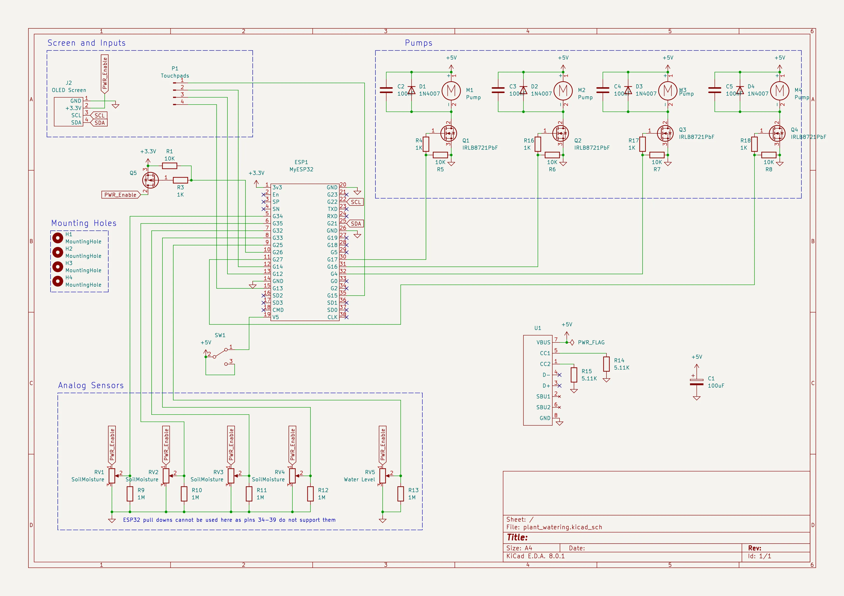
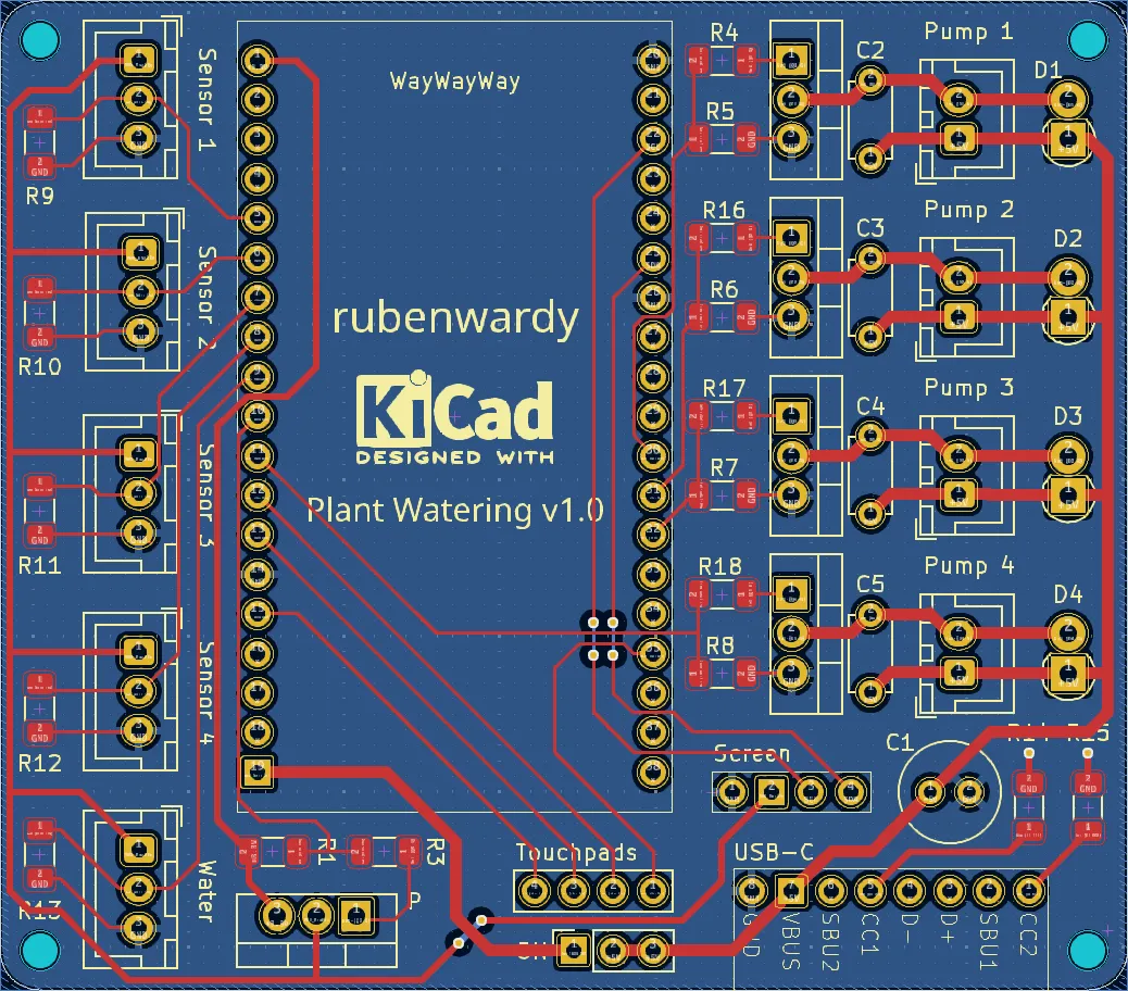
The next step is to turn this schematic into a PCB by placing components on a board design and connecting them according to the schematic. KiCAD ensures that the board design matches the schematic. This two-step process reduces mistakes.
Component selection #
My PCB uses two different methods to attach components to the board. The first is Through-Hole Technology (THT), where components are attached with wires that go through the board and are soldered to the other side. The second is Surface-Mount Device (SMD) or Surface-Mount Technology (SMT), where the component sits on top of the board and is soldered to pads on the board.
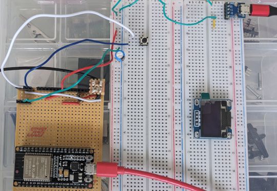
I chose to use a mixture of THT and SMD for different reasons. I used SMD for the resistors, as I wanted to practice soldering SMD components, and passive components like resistors are the simplest to work with. I used THT for the remaining components because I wanted to use the same components used in the breadboard prototype. Testing the circuit on a breadboard first reduces the risk of wasted time and money.
The components are:
- 1x ESP32-WROOM-32 dev board
- 4x pumps
- 4x capacitive soil moisture sensors
- Silicone tubing
- 4x N-Channel MOSFETs (IRLB8721, massively overspecced)
- 1x P-Channel MOSFET (I need to order one, currently bridging with a wire)
- 1x USB-C breakout
- 1x 100uF electrolytic capacitor
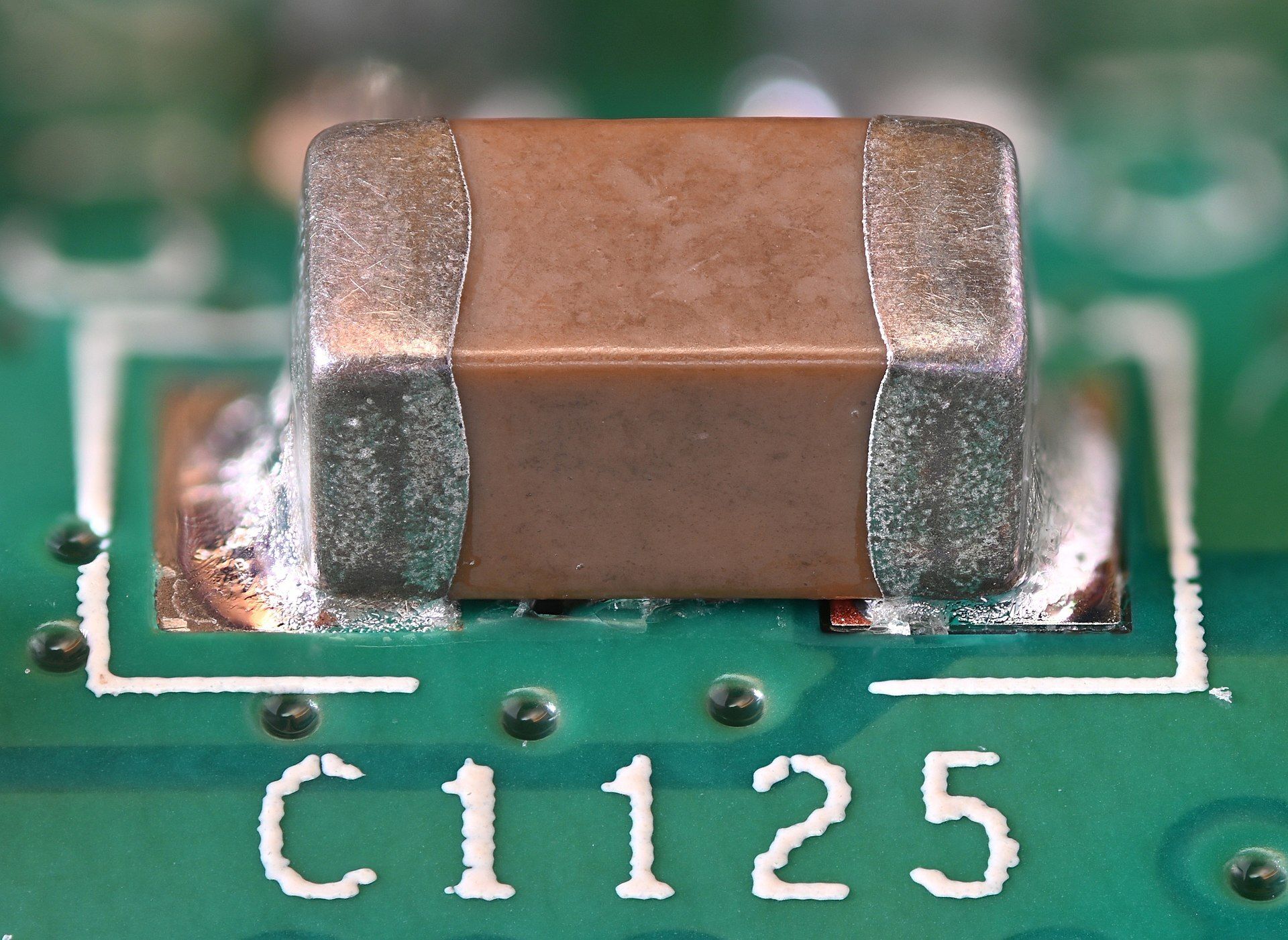
- 4x 100nF ceramic capacitors
- 4x diodes (1N4007)
- 5x JST 3-pin
- 4x JST 2-pin
- SMD resistors: 5x 10K, 5x 1M, 5x 1K, 2x 5.11K
Design lessons #
Before I ordered my PCB, I made sure to run the design by some experienced people and ask for feedback.
One beginner mistake I made was an overuse of right and acute angles when routing traces. Whilst less of a problem in modern fabrication, right and acute angles can trap etchant and cause issues with board manufacture.
I also had some unnecessary bridges. Remember that grounding video? It’s very important to minimise the number of breaks in the ground plane, especially under power and signal traces. I was able to move some components to remove all but a couple of ground breaks and vias.

USB-C support #
My PCB supports USB-C for power. I’m a big fan of USB-C, so it was nice to have this instead of Micro-USB like my previous projects. I followed a guide by PCBWay. It’s quite easy to implement for 5V power - you just need two CC resistors to set the voltage to 5V.
I used a breakout for the USB-C connector because I didn’t feel confident soldering the USB-C socket onto the board. The breakout doesn’t really add anything. On future boards, I’ll just solder a USB-C connector directly.
PCB assembly #
Once I was happy with my PCB’s design, I sent it to be produced by PCBWay. Not long after, I had five copies of the PCB on my desk.
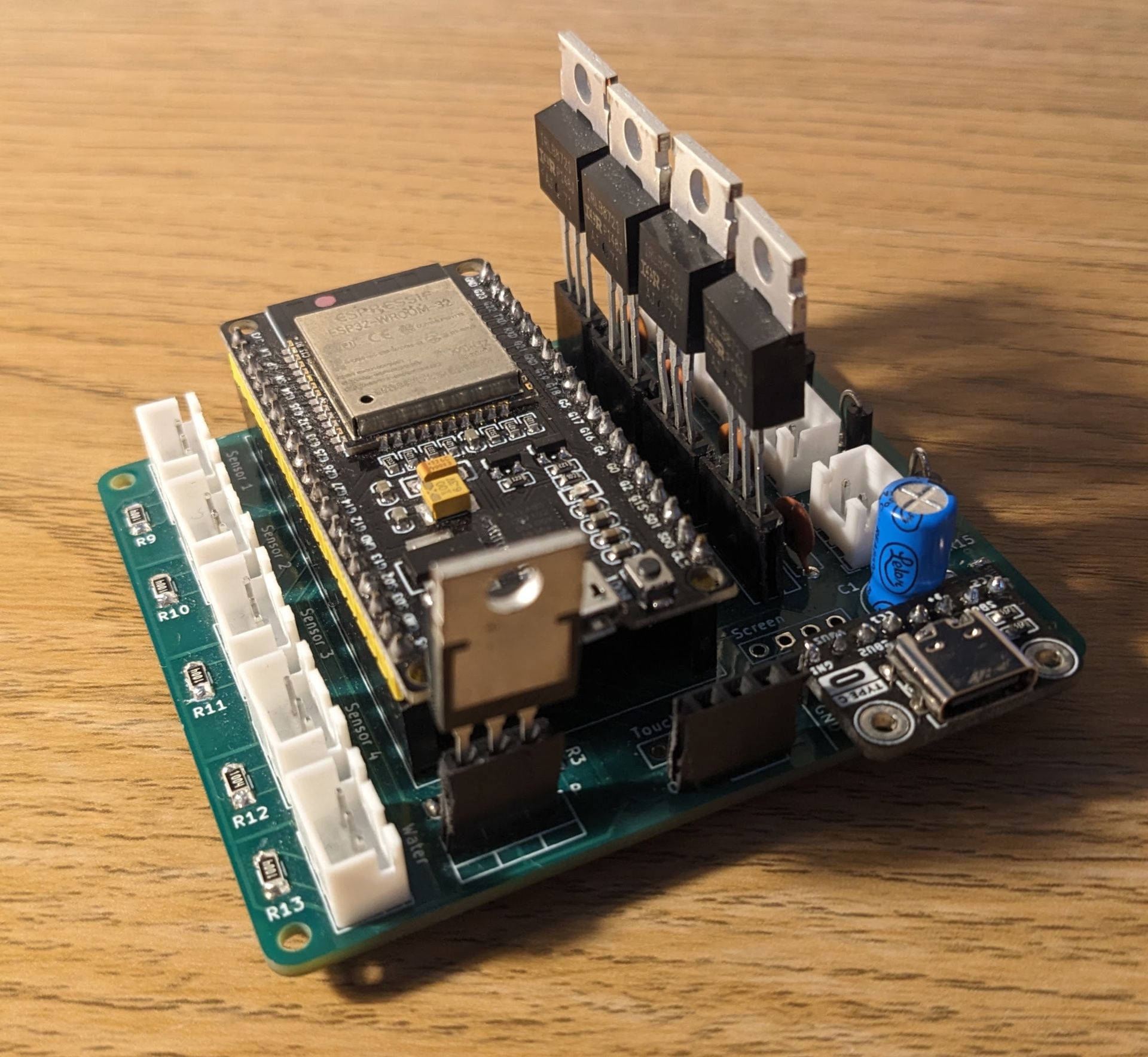
Before assembling my PCB, I practised soldering SMD components on a practice board I bought from the internet. I also used one of the five copies to practice soldering SMD resistors.
I started the assembly by soldering SMD resistors, checking with a multimeter as I went. I proceeded with the rest of the assembly in this manner - soldering on components and checking that they were connected correctly. I focused on getting a single pump up and working before I soldered the rest.
JST-XH #
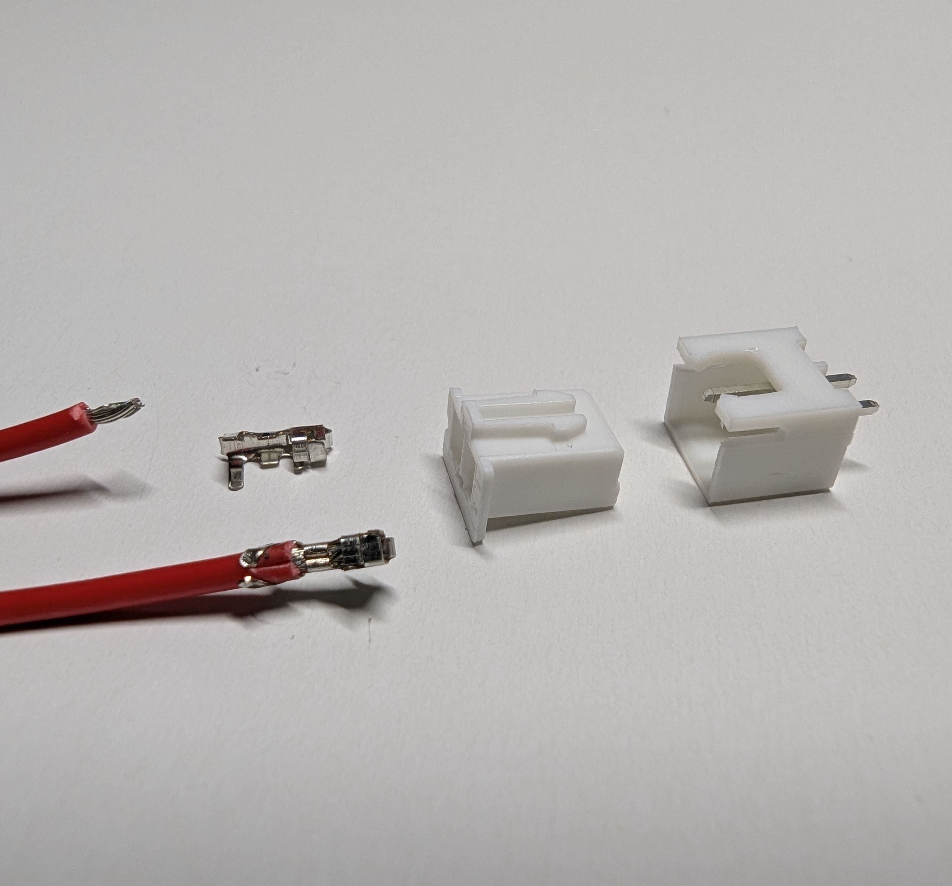
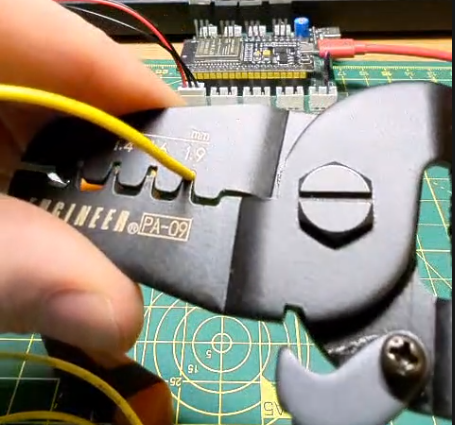
The pumps and sensors attach to the board using JST-XH connectors. By far the most challenging part of this project was creating these JST plugs.
I started by following a guide on YouTube that soldered the plugs. I found that the plugs never fit into the sockets correctly and were very fragile. This was especially a problem for the the thin gauge water pump wires.This one issue was very frustrating and caused me to shelve the project for almost two years.
In the end, I bought a crimping tool. It turns out that using the proper tool for a job is so much easier! The connectors are meant to be crimped using a tool and not soldered.
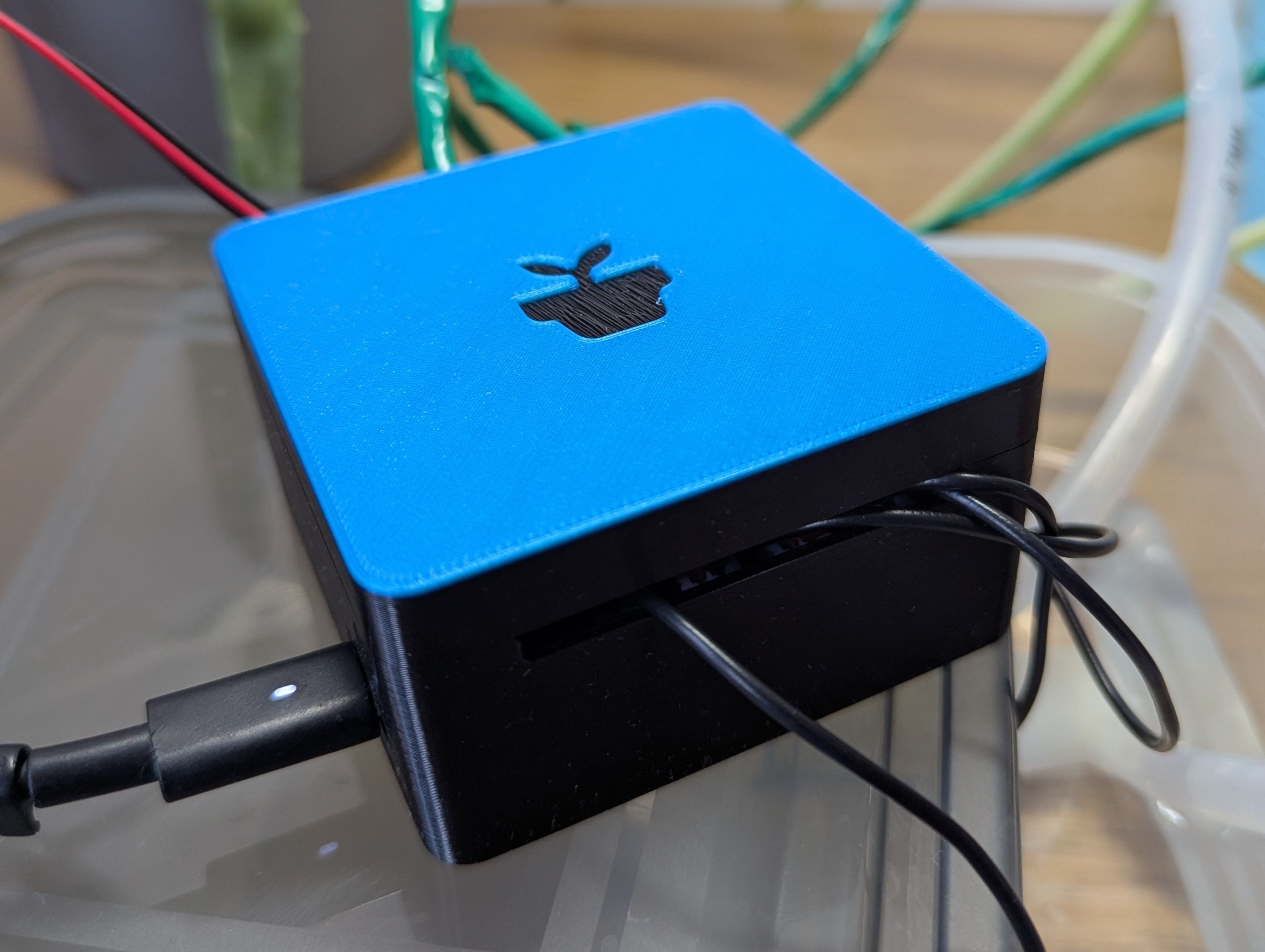
Final result #
I designed a simple enclosure and printed it using my Prusa Mini+. I use a plastic food container for the water tank, as 3d prints don’t tend to be watertight. I used an existing design by Emilostuff to clip the tubes onto the soil sensors.
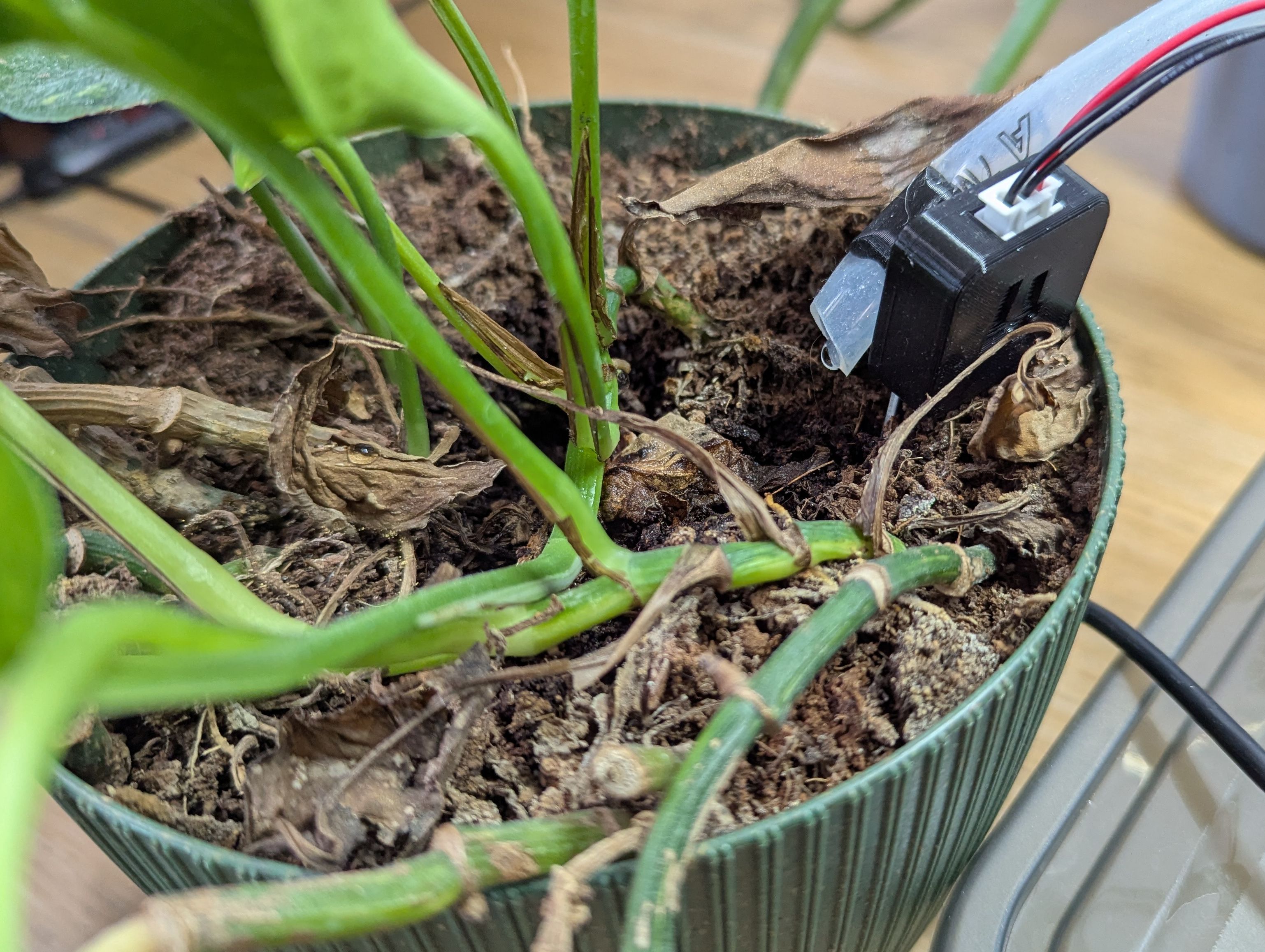
Here is the system connected to four plants:
Mistakes and future improvements #
Don’t use a pen lid on a soldering iron #
In case anyone is wondering, putting a pen lid on a soldering iron does not end well for the lid or fingers. I thought I was still holding my flux pen. It created a hole in the lid but luckily my fingers and the iron tip was fine.
Reduce size #
I choose to place the MOSFETs in headers to make it easier to replace them. This isn’t really necessary, and soldering the MOSFETs directly would make the design smaller.
A future design could use SMD MOSFETs and capacitors to allow the board to be even smaller.
JST connector wiring #
The order of the connections on the soil moisture sensor JST sockets does not match the order on the soil moisture sensor. This means that the wires need to cross over and also means the cable can only be plugged in one direction. Plugging the wrong end of the cable in could lead to damage.
The plant sensor wires are wrapped in electrical tape to keep the three wires together. This doesn’t look very professional, it would be nice to do this better.
Screen and input #
It would be nice to be able to interact with the system. The PCB has header pins for an OLED screen and four capacitive touch pads. There are also pins for an on-off switch.
Internet of Things integration #
I chose an ESP32 as it comes with WiFi built in. In the future, I’d like to connect the plant watering system to an open-source IoT dashboard. I like the idea of using an open protocol like MQTT for my devices.
Create a water tank #
I could attach the plant watering system to the tupperware lid, drilling holes for pipes and the pump wires. This would allow the container to be sealed and make the plant watering system a nice contained unit.
Conclusion #
I now know how to make PCBs! This is an exciting new skill to have. I’ve learned a lot by doing this project and have a lot of ideas for things to do next.
It’s a shame that the JST issue caused me to shelve this project for so long. Once I got around to using the crimping tool, it wasn’t that hard to finish up the project. I wish I had access to a maker space because I think that would have helped a lot, both with getting help and trying out tools.
Comments